
source: http://www.hardwaresecrets.com/article/Everything-You-Need-To-Know-About-DDR-DDR2-and-DDR3-Memories/167/1
Introduction
In this tutorial, we will explore the main technical differences between DDR, DDR2 and DDR3 memories. Enjoy!
Before we start going into the specifics, you need to know thatDDR, DDR2, and DDR3 are based on SDRAM (Synchronous Dynamic Random AccessMemory) design, meaning that they use a clock signal to synchronize things. DDRstands for Double Data Rate. Memories from this category transfer two datachunks per clock cycle. Translation: They achieve double the performance of memories without this feature running at the same clock rate (namely SDRAM memories, which are not available for PCs anymore).
Because of this feature,these memories are labeled with double the real maximum clock rate they canoperate. For example, DDR2-800 memories work at 400 MHz, DDR2-1066 and DDR3-1066 memories work at 533 MHz, DDR3-1333 memories work at 666.6 MHz, and so on.
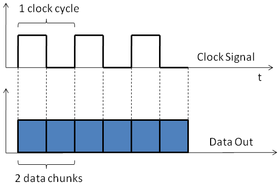
Figure 1: Clock signal and DDR mode
It is very important to understand that these clock rates arethe maximum the memory can officially use. This does not, by any means,guarantee that the memory will work at those “speeds” automatically. Forexample, if you install DDR2-1066 memories on a computer that can only (or itis wrongly configured to) access the memory subsystem at 400 MHz (800 MHz DDR),the memories will be accessed at 400 MHz (800 MHz DDR) and not at 533 MHz(1,066 MHz DDR). This happens because the clock signal is provided by thememory controller, a circuit that is located outside the memory (in the northbridge chip from the motherboard or embedded inside the CPU, depending on thesystem).
This naming system DDRx-yyyy (where x is the technology generation and yyyy is the DDR clock rate), in theory, is used only for the memory chips.The memory modules – the little printed circuit boards to where the memorychips are soldered – use a different naming system: PCx-zzzz, where x is the technology generation and zzzz is the maximum theoretical transfer rate (a.k.a.maximum bandwidth). This number tells us how many bytes can be transferredper second between the memory controller and the memory module, assuming thatdata will be transferred on every single clock pulse. This math is easily doneby multiplying the DDR clock in MHz by eight. (Actually, the real math is done by multiplying by 64 and then dividing by eight; since 64 / 8 =8, we can simply multiply by eight to achieve the same result.) This willgive us the maximum theoretical transfer rate in MB/s (megabytes per second).For example, DDR2-800 memories have a maximum theoretical transfer rate of6,400 MB/s (800 x 8), and memory modules using this kind of memory are called PC2-6400. In some cases, the number is rounded off. For example, DDR3-1333 memories have a maximum theoretical transfer rate of 10,666 MB/s. Memory modules using this kind of memory are called PC3-10666 or PC3-10600,depending on the manufacturer.
It is really important to understand that these numbers aremaximum theoretical numbers, and they are never reached. This occursbecause for the math, we are assuming that the memory will be sending data tothe memory controller every single clock cycle, which simply doesn’t happen.The memory controller and the memory need to exchange commands (for example, acommand instructing the memory to deliver data stored at a given position), andduring such time the memory won’t be transferring data.
Now that you know the basics about DDR memories,let’s talk about the specifics.
Speeds
One of the main differences between DDR, DDR2 and DDR3 is thehighest transfer rate each generation can reach. Below we list the most commonspeeds for each generation. Some manufacturers can deliver memory chips capableof achieving other speeds than those listed; for example, specialtymemories targeted to overclockers. Clocks ending in 33 and 66 MHz are, in fact,periodic decimal expansions (33.3333 and 66.6666, respectively).
Memory | Real Clock | Maximum Theoretical Transfer Rate | Memory Module |
DDR200 | 100 MHz | 1,600 MB/s | PC-1600 |
DDR266 | 133 MHz | 2,133 MB/s | PC-2100 |
DDR333 | 166 MHz | 2,666 MB/s | PC-2700 |
DDR400 | 200 MHz | 3,200 MB/s | PC-3200 |
DDR2-400 | 200 MHz | 3,200 MB/s | PC2-3200 |
DDR2-533 | 266 MHz | 4,266 MB/s | PC2-4200 |
DDR2-667 | 333 MHz | 5,333 MB/s | PC2-5300 |
DDR2-800 | 400 MHz | 6,400 MB/s | PC2-6400 |
DDR2-1066 | 533 MHz | 8,533 MB/s | PC2-8500 |
DDR3-800 | 400 MHz | 6,400 MB/s | PC3-6400 |
DDR3-1066 | 533 MHz | 8,500 MB/s | PC3-8500 |
DDR3-1333 | 666 MHz | 10,666 MB/s | PC3-10600 |
DDR3-1600 | 800 MHz | 12,800 MB/s | PC3-12800 |
Voltages
DDR3 memories operate at lower voltages compared to DDR2 memories,which in turn operate at lower voltages compared to DDR memories. This meansthat DDR3 memories consume less power than DDR2 memories, which in turn consumeless power than DDR memories.
Typically, DDR memories are fed with 2.5 V, DDR2 memories are fedwith 1.8 V, and DDR3 memories are fed with 1.5 V (although modules requiring1.6 V or 1.65 V are common, and chips requiring only 1.35 V may become commonin the future). Some memory modules may require higher voltages than thoselisted. This happens especially with memories supporting the operation at clockrates higher than the official ones (i.e., memories targeted to overclocking).
Technology | Typical Voltage |
DDR | 2.5 V |
DDR2 | 1.8 V |
DDR3 | 1.5 V |
Latency
Latency is the time the memory controller must wait betweenrequesting data and the actual delivery of them. It is also known as CAS(Column Address Strobe) Latency or simply CL. This number is expressed in termsof clock cycles. For example, a memory with CL3 means that the memorycontroller must wait three clock cycles until data is delivered after a requestis made. For a memory with CL5, the memory controller will have to waitlonger: five clock cycles. So you should always look for the memorymodules with the lowest latency possible.
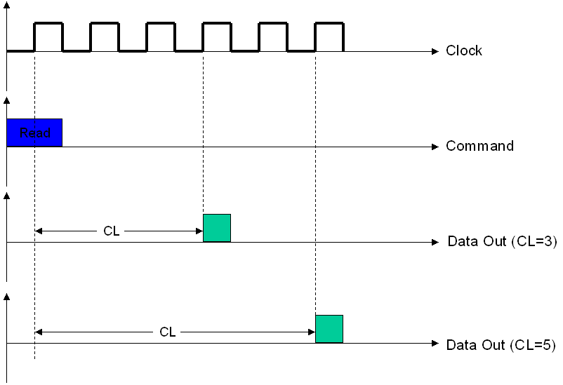
Figure 2: Latency
DDR3 memories have higher latencies than DDR2 memories, which inturn have higher latencies than DDR memories. DDR2 and DDR3 memories have anadditional parameter called AL (Additional Latency) or simply A. With DDR2 andDDR3 memories the total latency will be CL+AL. Fortunately, almost all DDR2 andDDR3 memories are AL 0, meaning that no additional latency is necessary. Belowwe summarize the most common latency values.
Technology | Typical Latency | Other Common Latencies Available |
DDR | 3 | 2, 2.5 |
DDR2 | 5 | 3, 4 |
DDR3 | 7 | 6, 8, 9 |
This means that DDR3 memories delay more clock cycles to startdelivering data compared to DDR2 memories (just like DDR2 memories delay moreclock cycles to start delivering data compared to DDR memories), but this doesnot necessarily mean a longer wait time (this will be true only whencomparing memories working at the exact same clock rate).
For example, a DDR2-800 CL5 memory will delay less time (i.e., isfaster) to start delivering data than a DDR3-800 CL7 memory. However, sinceboth are “800 MHz” memories, both provide the exact same maximum theoreticaltransfer rate (6,400 MB/s). Also, it is important to remember that the DDR3memory will consume less power than the DDR2.
When comparing modules with different clockrates, you need to do some math to be able to compare the latencies. Noticethat we are talking about “clock cycles.” When the clock is higher, each clockcycle is shorter (i.e., shorter period). For example, on a DDR2-800memory, each clock cycle takes 2.5 ns (1 ns = 0.000000001 second). Themath is simple: period = 1 / frequency. (Note that you need to use the realclock, not the DDR clock on this formula. To make things easier, wecompiled the reference table below.) The initial wait time ofa DDR2-800 memory with CL 5 corresponds to 12.5 ns (2.5 ns x 5). Nowsuppose we have a DDR3-1333 memory with CL 7. With this memory, each clockcycle will have a period of 1.5 ns (see table below), so the total wait time(latency) will be 10.5 ns (1.5 ns x 7). Even though the latency of thisDDR3 memory appears to be higher (7 vs. 5), the wait time is actually lower. Sodon’t go around thinking that DDR3 memories have worse latencies than DDR2memories; it will depend on the clock rate you are talking about.
DDR Clock | Real Clock | Clock Period |
200 MHz | 100 MHz | 10 ns |
266 MHz | 133 MHz | 7.5 ns |
333 MHz | 166 MHz | 6 ns |
400 MHz | 200 MHz | 5 ns |
533 MHz | 266 MHz | 3.75 ns |
666 MHz | 333 MHz | 3 ns |
800 MHz | 400 MHz | 2.5 ns |
1,066 MHz | 533 MHz | 1.875 ns |
1,333 MHz | 666 MHz | 1.5 ns |
1,600 MHz | 800 MHz | 1.25 ns |
Usually manufacturers announce the memory timings as a series ofseveral numbers separated by a dash (e.g., 5-5-5-5, 7-10-10-10, etc.). The CASlatency is always the first number from these series. See the examples onFigures 3 and 4. If you want to know what the other numbers mean, please readour tutorialUnderstanding RAM Timings.

Figure 3: DDR2-1066 with CL 5

Figure 4: DDR3-1066 with CL 7
Prefetch
Dynamic memories store data inside an array of tiny capacitors.DDR memories transfer two bits of data per clock cycle from the memory array tothe memory internal I/O buffer. This is called 2-bit prefetch. On DDR2 this internaldatapath was increased to four bits, and on DDR3 it was raised again to eightbits. This is actually the trick that allows DDR3 to work at higher clock ratesthan DDR2, and DDR2 at higher clock rates than DDR.
The clocks to which we have been referring so far arethe clock rates on the “external world,” i.e., on the I/O interface from thememory, where the communication between the memory and the memory controllertakes place. Internally, however, the memory works a little differently.
To better understand this idea, let’s compare a DDR-400, aDDR2-400 and a DDR3-400 memory chip. (We know that DDR3-400 memories don’texist, but pretend they do.) These three chips work externally at 200 MHztransferring two data per clock cycle, achieving an external performance as ifthey were working at 400 MHz. Internally, however, the DDR chip transfers twobits between the memory array and the I/O buffer, so to match the I/O interfacespeed this datapath has to work at 200 MHz (200 MHz x 2 = 400 MHz). Since on DDR2this datapath was increased from two bits to four bits, it can work at half theclock rate in order to achieve the same performance (100 MHz x 4 = 400 MHz).The same thing happens with DDR3. The datapath was doubled again to eight bits,so it can work at half the clock rate as DDR2 or only ¼ of the clock rate ofDDR in order to achieve the same performance (50 MHz x 8 = 400 MHz).
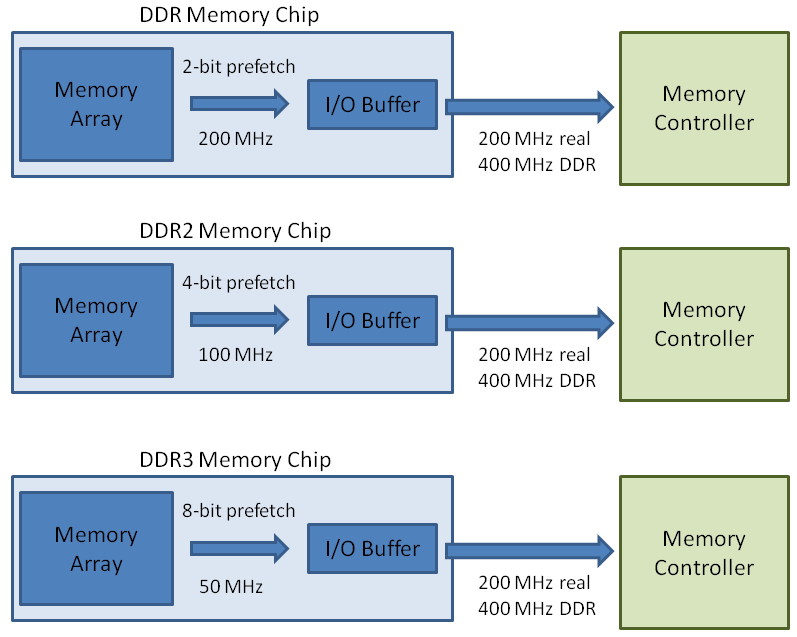
Figure 5: Understanding n-bit prefetching
Doubling the internaldatapath at each generation means that each new memory generation canpredictably have chip models with double the maximum clock rate achieved on theprevious one. For example, on DDR-400, DDR2-800 and DDR3-1600 memories thememory works internally at the same clock rate (200 MHz).
Resistive Termination
On DDR memories, the necessary resistive termination is located onthe motherboard, while on DDR2 and DDR3 memories this termination is locatedinside the memory chips – a technique called ODT (On-Die Termination).
This is done in order to make the signals “cleaner.” In Figure 5,you can see the signal that reaches the memory chip. On the left hand side yousee the signals on a system that uses motherboard termination (DDR memories),while on the right hand side you see the signals on a system that uses on-dietermination (DDR2 and DDR3 memories). Even a layman can easily see thatthe signals on the right-hand side are cleaner and are more stable than thesignals on the left-hand side. On the yellow square you can compare the timeframe difference; this time frame is the time the memory has to read orwrite a piece of data. With the use of on-die termination, this time frame gotwider, allowing higher clocks to be achieved since the memory has more time toread or write a data chunk.

Figure 6: Comparison between motherboard termination and on-die termination
Physical Aspect
Finally, we have thedifferences at the physical level. You buy memory chips already soldered on aprinted circuit board called a “memory module.” Memory modules for each DDRgeneration are physically different, so for example you won’t be able toinstall a DDR2 module in a DDR3 socket. Unless your motherboard supports bothDDR2 and DDR3 sockets (only a few do), you cannot upgrade from DDR2 to DDR3without replacing the motherboard and eventually the CPU (if in your system thememory controller is embedded in the CPU, as with all processors from AMDand Core i7 from Intel). The same thing is valid with DDR and DDR2. Other thanfor a few are rare exceptions, you cannot replace DDR memories with DDR2. DDR2and DDR3 modules have the same number of pins, however, the key notch is placedin a different position.
Memory Module | Number of Pins |
DDR | 184 |
DDR2 | 240 |
DDR3 | 240 |

Figure 7: Difference in edge contacts between DDR and DDR2

Figure 8: Difference in edge contacts between DDR2 and DDR3
All DDR2 and DDR3 chips use BGA (Ball Grid Array) packaging, whileDDR chips almost always use TSOP (Thin Small-Outline Package) packaging. Thereare a few DDR chips with BGA packaging on the market (like the ones fromKingmax), but they are uncommon. In Figure 9, you can see what a TSOP chipon a DDR module looks like, while in Figure 10 you can see what a BGA chipon a DDR2 looks like.

Figure 9: DDR chips almost always use TSOP packaging

Figure 10: DDR2 and DDR3 chips use BGA packaging