source: http://www.lostcircuits.com/mambo//index.php?option=com_content&task=view&id=35&Itemid=60
A very old article
Page 1 of 8
DDR (I) is approaching the end of its dominating role in the desktop space to be replaced by the second generation of double data rate memory starting at 400 MHz and using a conventional 64/72 bit parallel bus interface. Lower operating voltage, new features like on-die termination, off-chip driver calibration, Posted CAS and variable write latency sound intriguing but what is really lurking behind the new standard. We have seen claims of up to 72% power savings over DDR I and other miracle cures for any bandwidth issues faced by the PC industry. We have done the math ourselves found a few convenient errors in some of the manufacturer's descriptions of DDR2. Otherwise, DDR2 looks very promising but who will benefit in the end? If the DRAM makers have their way, DDR or DDR I as we know it will be succeeded at some point in the coming year by the next generation of mainstream SDRAM: DDR2 The second generation of DDR has been anticipated by consumers and DRAM manufacturers alike, however, for rather different reasons.
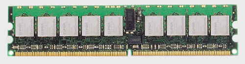
Hypothetical DDR2 Registered ECC DIMM using Elpida components (altered after Elpida). The pin count on the DIMM has increased from 184 pins in DDR (I) to 240 pins in the new DDR2 format.
Most consumers primarily associate higher performance with DDR2. Starting speed grades of 400 MHz data rate for system memory and already going up to 1 GHz in graphics applications, even before the new technology has hit the streets sound like some real progress has been made in DRAM technology. This is especially true in light of the difficulties in current DDR I technology to yield DDR400 MHz components in sufficient quantity.
So what are the magic ingredients that makes DDR2 wiggle so much faster than DDR I? More importantly, we have heard all the rumors of DDR2 being backward compatible with DDR I but we also heard the opposite. For the graphics card manufacturers, the compatibility may not be such a crucial factor but what will happen to the consumer who wants to upgrade his memory to DDR2 on an existing mainboard? Last not least, since there is no such thing as a free lunch, will DDR2 be more expensive than current DDR (I) or what other trade-offs will there be e.g. in terms of latency vs. bandwidth?
We have seen the wildest speculations about DDR2 floating on the web, including the use of very inventive math by some DRAM manufacturers to hi-light the benefits of the new standard. We have heard terms like "DDR2 in emulation mode" and "poor man's DDR", we have seen articles using all the correct buzz words albeit somewhat out of context. But what is really behind the new technology?
Page 2 of 8
Some Basics
Before we start with the magic, it is necessary to know a bit more about the ingredients in general. Each DRAM, regardless of whether it is asynchronous or synchronous (SDRAM) consists of basically two three components, that are:
- power supply
- Logic including I/O buffers
- DRAM array
Single Data SDRAM
In most DRAMs, the core and the I/O logic are running at the same frequency, regardless of whether we are looking at DRAM or SDRAM. In SDRAM each output buffer can relase a single bit per clock cycle. This bit is output on the rising edge of the clock.
DDR (I)
In DDR, every I/O buffer or short DQ (as in data queue) can output two bits per clock cycle. The prerequisite for this to happen, of course, is that two bits are available to be released. Consequently, each read command will transfer two bits from the array into the DQ. Since the data are fetched from the array before they are released, the memory parlance describes this as "prefetch of 2". The simplest way to conceptualize this is to use two separate data lines from the primary sense amps to the I/O buffers. The DQs are then outputting the data in a time multiplexed manner, meaning one bit at a time on the same output line. The easy way to do this is to collect the two bits in two separate pipeline stages and then release them in the order of the queue on the rising and the falling edge of the clock. Because two bits are released to the bus per pin and clock cycle, the protocol used is called double data rate or DDR.

Core frequency vs. I/O Buffer frequency vs. data rate in SDRAM, DDR 1 and DDR2
In all cases, the core is running at 100 MHz, in the case of SDRAM and DDR I, the I/O buffers are synchronous with the core, only the protocol varies and in the case of DDR2, the I/O buffers are clocked at twice the core frequency. In order to satisfy the output, DDR I prefetches 2 bits, DDR2 needs to prefetch four bits with every read command and pipeline them for time multiplexed output.
The Core as the Speed Limit
Ramping up the speed of the I/O buffers appears to be somewhat easier than increasing the speed of the core that makes about 90% of the total die. Reasons for the inherent slowness of the core is that it consists of capacitors that need to discharge their information, which then has to be sensed and amplified by the primary sense amplifiers before even a read command can be issued. In addition, the read is destructive, meaning that the capacitors or memory cells are emptied of their information which then has to be restored by writing them back to the cells, that is, restoring the original charge of each capacitor when the bank is closed.
The factors outlined above lead to the phenomenon of the minimum bank open (tRAS) and bank cycle (tRC) time where tRAS is the minimum time a bank has to stay open after the activate command before it can be precharged or closed again. tRC (Row Cycle time; Bank Cycle time) is the sum of tRAS (also called RAS Pulse Width) and tRP (Precharge Latency) and it solely depends on the speed of the core.
Historically, tRAS used to be defined as the sum of the RAS-to-CAS delay and the CAS latency, however, these conventions are waning in that the strobes are getting much faster than the sense amps and the potential build-up in the bit lines necessary to restore the data in the memory cells. Likewise, the output buffers and I/O registers are getting way ahead of the core speed.
Page 3 of 8
DDR2: Raising the Speed Limit
If it is the core that is holding back the DRAM operating frequency, we can simply stick two cores together and combine them with a single I/O path to double the output bandwidth. In reality, this is done by prefetching twice the number of bits from a single core but the principle is the same. The net result is a prefetch of four that are put into the appropriate registers and output one after another to the bus.
The only other thing that needs to be accomplished to manage the internal data flow increase is to double the clock on the I/O buffers so that they are running at twice the speed of the core. To sum this up, DDR2 400 will feature a 100 MHz (10 ns clock cycle; tCK) core and I/O buffers that are running at twice the frequency while outputting data using DDR mode. This results in output of four bits / clock which is equivalent to a quad pumped interface in terms of bandwidth.
From a core manufacturing standpoint, a DDR2 400 is equivalent to a PC1600 core whereas a DDR (I) 400 core has to be twice as fast. Since low cost is the one and only driving factor in the DRAM industry, it is a no-brainer which one the DRAM manufacturers will like. Coincidentally, at this year's Fall Intel Developer Forum, Micron introduced their new metric as bandwidth / $$ or was it $$ / bandwidth?
Power Issues
One huge problem with current DDR is power consumption. A desktop system featuring 4 GB of DDR will consume on every read some 35-40 W of memory power. Reducing the nominal operating voltage from 2.5V to 1.8V, will result in power savings of 28 %. At the same time, a reduced voltage swing allows higher frequencies.
Off-Chip Driver Calibration
Unfortunately, it is not that easy. It is true that lower voltage swings enable higher frequencies but after a certain point, the ramping of the voltages will show a significant skew. The skew can be reduced by increased drive strength, however, with the drawback of a voltage overshoot / undershoot at the rising and falling edges, respectively. One additional problem with high frequency signalling is the phenomenon of trace delays. The solution in DDR was to add clock forwarding in form of a simple data strobe. DDR2 takes things further by introducing a bidirectional, differential I/O buffer strobe consisting of DQS and /DQS as signals. Differential means that the two signals are measured against each other instead of using a simple strobe signal and a reference point. In theory the pull-up and pull-down signals should be mirror-symmetric to each other but reality shows otherwise. That means that there will be skew-induced delays to reaching the output high and low voltages (VOH and VOL) and the cross points between DQS and /DQS used for clock forwarding will not necessarily coincide with the DQ crossing the reference voltage (Vref) or even be consistent from one clock to the next. The mismatch between clock and data reference points is referred to as the DQ-DQS skew.
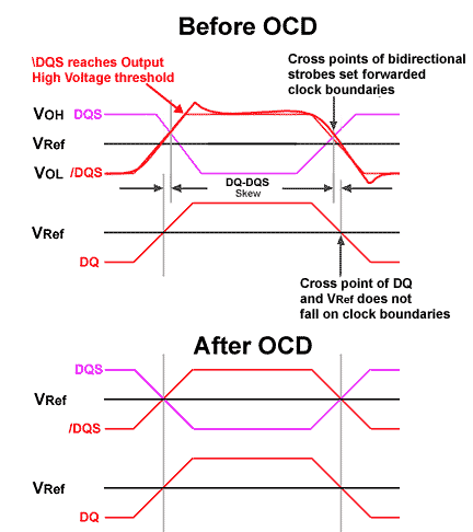
Clock-Forwarding and OCD-calibration
DQS and DQ traces will never be a perfect square function, the slope of the voltage ramp relative to the clock cycle time will get shallower with increasing frequency. Increasing the signal strength results in voltage over- and undershoots. For simplicity reasons, we have drawn only one "real life" strobe signal and substituted simplified traces for the remaining signals. Simplified traces means that we use the point where the voltage reaches the High or Low Output enable threshold. Disregarding all jittter, in the upper part of the figure, DQS and /DQS are still unequal which results in shifting of their cross point. Since the cross point defines the source synchronous clocking or forwarded clock boundary, a mismatch between the external clock and the data clock will occur. This mismatch is the DQ-DQS skew which causes deterioration of the data integrity.
The lower half of the figure shows the hypothetical result of OCD calibration where all signals are matching perfectly. Every marketing person would give their first born for real traces as clean as those shown here, though.
In addition, while the input impedances of most I/O buffers on a single chip are usually in the same order, there can be slight differences between the individual DQs that make it difficult to find the all-encompassing formula. If different designs from different vendors have to be taken into account, the situation gets far more difficult.
One way to solve the problem is to use Off-Chip Driver calibration (OCD calibration) where both parts of the differential strobes are calibrated against each other and against the DQ signal. Through this sort of calibration, the ramping voltages are optimized for the buffer impedances to reduce over and undershooting at the rising and falling edges. More importantly, DQS and /DQS are matched so that their cross point coincides with the DQ signal crossing the reference voltage to eliminate DQ-DQS skew. In summary, the entire scheme results in better compatibility between different designs, higher signal integrity through minimization of DQ-DQS skew and reduced overshoot / undershoot for better signal quality.
BGA vs. TSOP
Probably the most overhyped and mis-interpreted aspect of DDR2 is the migration from TSOP to a BGA interface with the argument that the little TSOP feet have too much resistance and inductivity / impedance and that the BGA interface will solve these problems. Keep in mind that the caliber of the TSOP feet is still orders of magnitude larger than the PCB traces. Keep in mind further that the package contacts still have to connect via bond wires to the actual pads on the die. Bond wires are typically 30 µm in diameter and compared to their resistance / impedance, the question of TSOP vs BGA becomes almost non-existent.
That does not mean that BGA has no advantages, on the contrary. However, the advantages are in the better control of signal integrity and easier calibration. Suffice it to say that with a standard design of DDR I without OCD-calibration, the benefit of BGA packaging is borderline measurable. However, it appears as if BGA is a prerequisite for OCD-calibration.
Page 4 of 8
On Die Termination (ODT)
Any pulse or signal propagating along a bus will reflect from any part that is different. This lapidary statement implies that as long as the bus traces are homogeneous and of infinite length, no signal reflection will occur. Such a bus would, however, be useless, because it would not have any target. Any target would be different by definition and, thus, cause signal reflections one way or another. Depending on the signal strength, and the ratio between the actual signal and the reflected mirror image, the two signals may cancel each other out or cause some other interferences. Therefore, it is mandatory to keep any reflections as small as possible.
The technical solution is termination of the signal, meaning that at the end of the signal path, a resistor to ground, VSS or VTT, depending on which nomenclature is used will simply swallow the signaling voltage which, therefore cannot be reflected. A termination resistor is comparable to a black hole where everything is going in but nothing is coming back out.
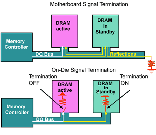
Classic mainboard termination of signal to eliminate reflections compared to on die termination (ODT). Shown is only the data bus, however, ODT can be activated for the clock forwarding strobes (DQS. /DQS) and the write data masks (DQM) as well, depending on the scheme selected by the controller.
Of course, there are risks associated with overly effective termination, that is, the signal can be absorbed without reaching the target, simply because the resistance of the terminator is too low. Therefore, termination resistor values are usually defined within very narrow margins.
In the case of DDR memory, we have repeatedly pointed out the location of the resistors that are usually aligned in a row parallel to and on the far side of the DIMM slots. The position can vary but that depends mostly on the trace routing on the mainboard. We have also shown on occasion that changing the value of the termination resistors, even within the specs allowed by the chipset manufacturer can result in different performance / overclocking characteristics of the system from one board revision to the next.
It is important to realize that signal reflection will only affect active components within the system. Even though this point is trivial, another trivia is that reflections will occur on active and non-active component interfaces. The current scheme of mainboard-based termination will absorb reflections at the end of the traces, however, reflections caused at the I/O interface to the memory chips will have to re-enter the bus first before they can be terminated. In other words, there is a constant noise level on the bus that will interfere with the data signals and cause quality degradation.
The elegant way out of this dilemma is to use what is called On-Die-Termination or ODT by adding a current sink to ground on the die itself. In order to preserve signal strength on the active bank, it is best to add a switch to turn off ODT simultaneously with enabling chip select. This way, all chips that are not selected for data I/O, that is, those that are in active standby mode will have ODT switched On to eliminate reflection where it originates, that is, at the bus to die interface. As a result, there is no possibility for the reflections to reenter the bus and contaminate the real signals. ODT can be used for the data I/O bus, the clock forwarding strobes and the write data masks (DQM) independent of each other as specified by the controller.
Page 5 of 8
Posted CAS and Additive Latency (AL)
For the DRAM designer and those who work on memory controllers, it is self-understood that the command bus can carry only one signal at the time. The same holds for the time-multiplexed address bus but at this point, we are only concerned with the command bus. Essentially, there are four command lines that are important, that is RAS, CAS, Chip Select (CS) and Write Enable (WE). Leaving CS out of the picture for now (since it only selects the physical bank out of all DIMMs within the system), any combination of high and low signals on the RAS, CAS and WE lines means either a bank activate (ACT), read, write, precharge or refresh command to name those commands important for the following. Typical command signals for the three lines mentioned above would be e.g. 101 or 110 or 010 using the RAS, CAS and WE line matrix. Keep in mind that we are talking about physical lines from separate pins on the controller to separate pins on the DRAM.
It is important to understand that only one command can be issued at any time because each of the three command lines can only be either high or low. Any two commands issued on the same clock will cause bus contention and so-called data collision (since at least one line would need to be high and low at the same time). For example, in bank interleave mode, a bank activate command to a second or third internal bank on the DRAM chip can be issued after the specified Row-To-Row Delay (tRRD). At the same time, because of a pre-defined RAS-To-CAS delay, a read command is already scheduled. The two commands coincide on the same clock and conflict or collide with each other on the command bus. Consequently, the next bank activate command will have to be pushed out by one cycle.
The bank activate is the first step in every memory access and, therefore, all subsequent steps like a read command to the same bank will be pushed out by the same 1 clock. Whatever terrain has been lost on the bank activate cannot be gained back by a faster CAS latency (it is impossible to change CAS latency on demand) and, therefore, there will be a gap or bubble in the data stream which will manifest itself in a memory bandwidth performance hit. We don't like performance hits, don't we?
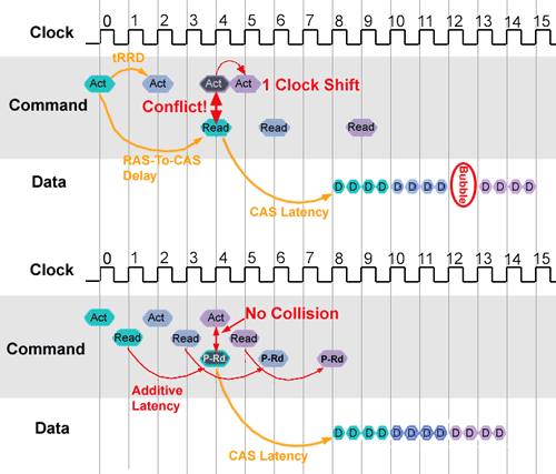
Conventional command issuing (top) compared to Posted CAS mode (bottom)
Out of the four internal banks accessible in bank interleave mode, three are shown in green, blue and purple (commands and resulting data). The clock traces refer to the I/O buffers, not to the core. Act: Bank activate command; Read: Read Command; P-Rd: Posted Read / Posted CAS; D: data output (1 bit/pin, 1 quadword / bus width).
Conventional Operation: Bank activate commands to internal banks are given with a Row-to-Row delay (tRRD) of 2. In this particular case, tRCD, i.e., the delay until a read command can be given, equals 4T. That means that the first read command (four cycles after the first bank activate) will fall onto the same clock as the third bank activate, in other words, the commands conflict with each other or collide on the bus. Consequently, one of the commands needs to be shifted by one clock. Since tRCD is defined in the BIOS setup, whereas bank activate commands are issued whenever a memory access is started, it is the bank activate that will be postponed. Bank activate, however, is the one command at the beginning of every access and, therefore, all subsequent commands to the same bank will be delayed by one cycle as well. This causes a bubble in the data stream. CAS latency equals four cycles here (20 or 15 ns for DDR400 or DDR533, respectively)
Posted CAS Operation: Bank activate and read commands (CAS) to the same bank are issued by the controller in back-to-back mode on consecutive cycles. In this case, all activate commands are done on even cycles whereas the read commands are always on odd cycles. Internally, the read commands (CAS commands) are held and then issued after a predefined additive latency (AL) as a postponed read (P-Rd) or Posted CAS. Since the Posted CAS does not require any external command, the bus is free to communicate a new activate command on the same clock. In summary, instead of a normal tRCD, we have a single cycle delay for the read command to which we need to add the internal delay (hence the name additive latency; AL) for the equivalent of a RAS-To-CAS delay and with no need for an additional read command. This will avoid bus collision.
The solution to this problem is to issue the commands in form of bundles, that is, a read command is issued immediately on the next cycle after the bank activate command that it belongs to. A command buffer on the DRAM chip will hold the command and internally schedule it without any further input needed from the command bus. This means that the command bus is free to activate another bank. This mode of operation, using an early issued but internally postponed read (or CAS) command is called Posted CAS where the delay or additive latency (AL) is specified by the mode register set (MRS) during initialization of the DRAM chip.
The consequence is that bank activate and read commands that belong together can be issued on consecutive clock cycles and immediately thereafter free up the bus for the next frame information structure (oops, that was serial ATA). The net effect of Posted CAS and AL is that there will be no command bus collisions and, thus, no bubbles in the data stream.
Update
Posted CAS and Additive Latency are optional features that are supported by the DRAM devices but do not necessarily have to be used by any given controller. IBM's memory controllers are apparently using Posted CAS and AL, likewise, the features appear to be used in graphics cards. However, to the best of our knowledge, neither Intel, nVidia, ATI or AMD are using Posted CAS / AL on mainstream chipsets for the PC-Workstation platform. In this case, the AL feature is simply set to "0" and a conventional Read command is given after tRCD has been satisfied.
Variable Write Latency
Conventional SDRAM including DDR I uses random accesses as the name implies. This means that the controller is free to write to any location within the physical memory space, which, in most cases, means that it will write to whichever page is open and to the column address closest to the (CAS) strobe. The result is a write latency of 1T, as opposed to read or CAS-Latency values of 2, 2.5 or 3. In DDR2, this changes in that the write latency will be the Read Latency (RL) minus 1T.
That means that at CAS-4, and AL-3 for a combined read latency of RL=7, the write latency will be 6T. This sounds somewhat worse than it is, especially compared to the 1T in DDR I but one needs to consider that, just like a read command, a write command will be issued early and will be using Posted CAS. That is, the write command abides by the same rules as the read command, only that the "Write Enable" signal is a logical "true" in this case. Effectively, therefore, the CAS latency is the important timing parameter to determine write latency, meaning that in the above example, the write latency will be 3T. This is only 3 times as long as the equivalent latency in DDR I. It will be very interesting to look at integrated graphics using UMA and DDR2 but it appears as if interesting is spelled u g l y.
Page 6 of 8
Backwards Compatibility
Depending on who is talking, DDR2 will be either compatible or incompatible with DDR I. To make it short, compatibility is limited to the basic command set, that is, the codes for read, write or similar commands have not been altered. Likewise, the basic device timings remain the same. However, this is as far as compatibility goes, meaning that aside from hypothetically understanding the same commands, there is no practical compatibility.
As we mentioned on the first page of this review, DDR2 DIMMs will feature 240 pins instead of 184 pins in DDR I, also, there are new functions that are not supported in DDR I but without which DDR2 devices will not function (ODT, OCD-calibration, Posted CAS and AL, variable write latency). Moreover, the voltage interface is different, 1.8V will not drive a 2.5V DIMM and vice versa it might become a substitute for a cold cathode case lighting. Briefly, that is.
All Key Features At One Glance
| DDR-I | DDR-II |
Frequency Specs | ||
Data Rate | 200/266/333/400 Mbps* | 400/533/(667) Mbps* |
Bus Frequency | 100/133/166/200 MHz | 200/266/(333) MHz |
DRAM Core Frequency | 100/133/166/200 MHz | 100/133/(166) MHz |
Prefetch Size | 2 bit | 4 bit |
Burst Length | 2/4/8 | 4/8** |
Data Strobe | Single DQS | Differential Strobe: DQS, /DQS*** |
CAS Latency | 1.5, 2, 2.5 | 3+, 4, 5 |
Write Latency | 1T | Read Latency-1 |
Power Specs | ||
Core Voltage (VDD) | 2.5V++ | 1.8V |
I/O Voltage (VDDQ) | SSTL_2 (2.5V) | SSTL_1.8 (1.8V) |
Format | ||
Packaging | TSOP (II), TBGA | FBGA |
Compatibility With DDR I | ||
Command Set | | Same as DDR I |
Basic Timing Parameters | | Same as DDR I |
Bus Utilization and Signal Integrity | ||
New Features | | ODT OCD-calibration Posted CAS Additive Latency+++ |
* Megabit/pin/sec
** The original BL was defined as 4 QW, however, a burst of 8 QW has been added as far as we know per request of Intel/Samsung.
*** DDR I only uses a single DQS, using the cross point with the reference voltage. DDR2 uses a differential DQS as shown on page 3.
+ CAS-3 is possible using a 533 MHz CAS-4 speed bin in DDR400 mode.
++ All current DDR I components are running at 1.8V internally, using voltage regulators to reduce VDD from 2.5V to 1.8V.
+++ Additive Latency can be 0,1,2,3,4T, the actual Read Latency is the sum of CAS latency and Additive Latency, e.g. CAS-4 + AL-4 =8T Read Latency.
Page 7 of 8
The Grand Picture
It is cheap, it offers a lot of bandwidth and nothing will ever be like it was before. Low power is a great accomplishment, higher density chips will be a side product and the wealth of new features like OCD-calibration, differential clock forwarding and ODT spell innovation. Different form factors, mechanical and electrical interfaces as well as differences in the command sets eliminate any backward compatibility between DDR2 and DDR I, at least for the end user but that's what is called progress and the same happened with the migration from SDRAM to DDR so we don't complain. Is DDR2 going to be the solution for high speed memory? We think yes but in all the marketing hype of DDR2, there are enough points that are being played down by the DRAM manufacturers.
Latencies
Overall data throughput depends on bandwidth and latencies. Peak bandwidth is important for certain applications that employ mostly streaming memory transfers. Other applications with more random accesses will get more mileage out of low latencies. There are different types of latency, from looking at the timing diagram two pages ago, it is obvious that there is little or no impact of the read or CAS latency on overall bandwidth as long as the controller stays in page and can employ bank interleaving.
However, the graph also shows something else and that is the initial access time (tRAC) that, in this case, is 8 cycles until the first data pop out. Eight cycles are the sum of tRCD plus CAS latency that are given as 20 ns (4 cycles) and 4 cycles each in the DDR2 product description of Samsung (weren't they the ones who were heralding DDR2 anyway?). These initial access latencies amount to exactly the same as what we got rid off a few years ago when PC-100 memory became obsolete. With DDR533 parts, we are looking at CAS-4 or CAS-5 with the higher speed bin potentially being able of running DDR400 in 3:3:3 mode. No matter which way one looks at it, the entire specs have the word latencies written all over them in fat, bold, neon, blinking letters. This is just the beginning of the story, though.
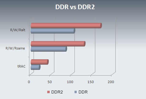
Not everybody here is familiar with timing diagrams and to sum up a few latencies and their effects on overall performance, we have simply calculated times required for certain transactions in DDR I 400 (2:2:2; not an official spec but we have been able to run at this speed for months already) and DDR2 400 (4:4:4). tRAC is the initial access latency, that is the time after a bank activate until the first word is output, shorter is better and there is little doubt which technology will take the lead. Initial access latency is one issue but there are other relevant scenarios. Common situations will be Read (BL=4) / Write / Read (BL=4) sequences where the second read can either fall into the same page or else be a page miss and go to an alternate page. The number of transactions in both cases will be the same, that is eight reads and 1 write. We assume the same read-write turnaround latency of 2T for both DDR I and DDR2 (even though this may favor DDR2) and the same data phase latency (delay after a write until a read command can be issued) of 3T. As we said, lower or shorter is better. The actual bandwidth will be the number of transactions (9 each) / ns. Keep in mind that we do not count CPU and address decode latencies on the chipset level in this case, neither are we considering single random reads (see below).
Single data SDRAM is capable of doing a burst of 1 (totally random, single bit read), bursts of 2, 4, 8 or full page. DDR I can do bursts of 2, 4 or 8. Because of the possibility of bank interleaving, we don't care too much about the full page burst but what happened to the burst of 1? The answer is quite simple, it is possible in theory but in reality we have a prefetch of 2 and, thus, yes, we can do a burst of 1 and throw away the second bit or quadword but we will not gain anything from it except for a hole in the transfer.
With DDR2, the prefetch of 4 and the double speed I/O buffers, we are looking at a much bigger bubble, that is, in case a single random read is needed, by definition, the bus utilization cannot be more than 25%. From the hole in the head perspective, we are dealing with 75% of waste in this scenario. Did we mention the word "ugly" before?
Bottom line is that there are applications where DDR2 appears to be somewhat unsuitable. A very obvious scenario is the server market where more than 95% of all memory accesses are random. Take a DDR2-equipped server and compare it with an EDO machine and guess which one will take the lead in daily operations. Honestly, we don't know, which is why we are putting up this challenge.
Another scenario is the united memory architecture. We have been looking at performance degradation and enhancements depending on resolution and latencies and the very clear message is that the importance of latencies will increase in a proportional fashion with resolution. What that means is that at low (e.g. 800 x 600 x 16) resolution, it is still possible to do away with high latencies, however, already at 1024 x 768 x 32, shaving off of a single latency cycle can cause as much as a 50% performance increase in 3D applications.
Page 8 of 8
DDR2 400, 533, The Stillborn Twins?
To make a long story short, there is a sudden, renewed interest at Intel in pushing DDR I to mainstream DDR400 and beyond, which looks like somebody finally did their homework. New speed bins on the DDR I roadmap encompass DDR I 533 which makes DDR2 400 and 533 obsolete products before they even hit the market and only leave DDR2 667 as marketable solution. Technical realization of DDR I 533 may require borrowing from DDR2 some features like ODT to provide cleaner signals.
Aggravating for a potential move towards DDR2 in this situation is the fact that DDR I took longer than expected to conquer the market, meaning that the industry is reluctant to abandon the current design in favor of yet another form factor. This is a very valid consideration, especially in view of the performance drawbacks with DDR2 and the fact that DDR I turned out to be much better than what it was originally designed for (PC2100).
Some Of Them Will Sing The Blues
Looking at the DRAM industry and the present offerings of DDR components we have to make the assumption that future success will not be something that can be pulled out of the magic hat like the white rabbit. Rather we have to assume that the manufacturers currently providing the highest performance discretes will be able to further extend their leading role into the realm of high speed DDR I and also profit from their technological leadership. Currently, the top performer is Winbond with their almost unchallenged -5 parts that have been shown to run up to 500 MHz data rate already on a DIMM. Second in line is Mosel Vitelic with their DDR400 components that currently don't reach the luxurious frequencies of Winbond chips but excel at low latency operation beyond 400 MHz data rate.
Next down are the Koreans, with both Samsung and Hynix offering solid DDR 400-capable product even though the current D-revision of Samsung chip still cannot close the gap to the almost legendary C-revision dies from a few months ago. Maybe it is time to rescussitate the old photo masks again. Hynix appears to have another Ace up their sleeve in the form of high density dies, we have not seen those yet so we will not give them serious consideration at this point. Elpida (for the record, they are not Korean but Japanese) is a somewhat unknown factor in the equation, we really don't know what their current capabilities are but we trust Inokai San and his staff to be on track.
Micron at this point has not been able to follow up on the success of their original PC2100 DDR chips, quite a few of which were capable of running up to 200/400 MHz on a DIMM. Moreover, according to the last IDF presentation, DDR400 yields are somewhat low which was one of the reasons for Micron to push DDR2.
Last not least, there is Infineon. Granted that they always spec their parts conservatively, we have yet to see any of their components that would run in PC3200 mode, chances are, though, that we just never got them. Still, most products listed on the Infineon website are DDR200 and 266 components with only a few sporadic offerings of DDR 333.
Between Intel And AMD
An interesting tidbit on the side is that Intel's P4 architecture, using all kinds of optimizations, including hardware-based dynamic speculative precomputing for branch-prediction and prefetching will be hurt less than AMD by the high latencies of DDR2. To spin this a bit further, the main advantage of AMD's Hammer architecture is the integration of the memory controller onto the CPU with the goal of reducing chipset-related (control and address decode) latencies. It only requires second grade math skills to see that shaving off one cycle out of nine (1/9) on the controller level for an initial access will yield less performance gain than reducing latencies by one cycle out of five (1/5) .
The difference between AMD and Intel, though, is that Intel is actively participating in defining (say: "bullying") the memory specifications of the future regardless of the cost concerns of the DRAMurai. AMD, on the other hand, whenever we asked them, appeared to be mostly concerned with staying mainstream and swallowing whatever was served by the DRAM makers as the best roadmap. Clearly, with helping the memory industry to make the cheapest possible DRAM, AMD will not win performance or market share. Intel has learned this lesson many years ago, and even though Rambus faltered in the end, Intel got more mileage out of them than anybody will ever admit. VIA Technologies are pursuing QBM (quad band memory, invented and heralded by Kentron) with high bandwidth and low latencies, and where is AMD?
Realistically, there is a solution for AMD. Low latency processors and controllers require low latency memory. It is as easy as that and we ........ well, we do have some suggestions.
(to be continued some two years down the road)
Update
In June 2006, AMD finally took the plunge and released the AM2 platform with support for DDR2 memory. The new socket interface is another iteration of a Socket 940. The move to DDR2 was facilitiated by the release of DDR2-800 at 4:4:4 latencies, which effectively provides the same access times as a PC3200 DDR(1) running at 2:2:2. Moreover, DDR2 puts less load on the address and control buses and supports higher density components, so that the current mainstream modules are boasting 1 GB module density divided over 2 ranks. High-end DDR2 modules are currently pushing 1200 MHz data rates at 5:5:5 latency settings and are offered by OCZ Technology and Corsair.